
|
|
|
PCB Symposium 2003 in Malaysia |
|
|
 |
| Japan: Country
report from Japan |
|
|
|
Country report from Japan
The Japan Offspring Fund
Mami Niida
Thank you, Chairman. I am Mami Niida from the Japan Offspring
Fund. It is a great pleasure to be able to hold such a big symposium
on PCB issue. I would like to thank you all.
The use of PCB
Japan has imported 1048 and tons and exported 5318 tons
of PCBs before the ban of production. Considering the amount
produced inside the country, 54001 tons are estimated to
have been used in Japan with 70% of them as in electric
equipments.
This table shows the kind of articles that contain PCBs.
PCBs were used in transformers in a building and railways,
capacitors in florescent lights, insulating oil in capacitors,
heat medium in heating articles, lubricating oil of pumps,
flame-resistant finish, non-carbon papers. They are also
reported to have been used in sealants of a building.
Uses
|
Product or
Place
|
| Insulating
oil |
Transformer |
Transformer of building, hospital,
railroad and ship |
| Condenser |
Capacitor of fluorecent right
and mercury right, air conditioning, washing machine,
black white television, microwave/ Fixed paper
condencer/ D.C. condencer/ Condencer for storage |
| Heating medium
(Heating and Cooling) |
Heating and cooling for chemical
industry, food industru and synthetic resin/ Preheating
of fuel oil on ship/ Central heating/ Panel heater |
| Lubricating oil
|
Lubricating oil for high temperature/
Vacumu pomp etc. |
Plasticizer
|
For insulating
|
Insulating tape |
For fire retaldant
|
Polyester resin/ Polyethirene
resin/ Rubber |
Others
|
Adhesive/ Varnis and wax/
Mix in asphalt |
| Copy |
Non carbonic papers (solvents),
electronic type copying papers |
| Paint and Ink
|
Paint on fire retaldant/ Paint
on corrosion resistant/ Paint on chemical/ Paint
on water proof/ Ink |
| Others
|
Coating on paper/ Sealant
of car/ Painting of pottery and grass/ Parts of
color televison/ Additive in pesticide/ Additive
in gasoline |
|
Reference: Ministry of Environment protection
in Japan (2001) The pamphlet (Japanese)
As you can see, PCBs were used in various equipments.
I would like to speak about the process of PCBs usage and
the following process of regulation.
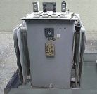
Transformer |
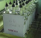
Condenser |
Capacitor |
The history of PCBs in Japan
In Japan, the production of PCBs started in 1954 by Kaneka
Corporation. They were named Kanechlor and depending on
their composition, were called KC-300, KC-600, etc. PCBs
had advantageous characteristics for industrial uses; they
could be used as insulators, they also were durable to heat.
It is considered that approximately 59000 tons were produced.
However, the Kanemi Yusho Case in 1968 provoked an attention
to the poisonous effects of PCBs. People who consumed rice
oil contaminated with PCBs became ill. It is said that approximately
14000 people have claimed to been poisoned at that time.
However, only about 1900 people were certified as victims
by the government. Certified and uncertified victims are
suffering from the after-effects. Recently, the media reported
that female victim tend to have disorders in reproductive
organs, and also have higher risk of miscarriage and stillbirth.
Although 35 years have passed, Kanemi Yusho Case is not
over.
In the study conducted later, it became clear that PCDF,
one kind of dioxin contained in PCB, was more poisonous
than PCB itself. However the poisonous features of PCBs
were strongly focused and became a social issue right after
the Kanemi Yusho Case, and subsequent regulations were made.
First of all, in 1972, an administrative guidance by the
Japanese Ministry of International Trade and Industry requested
the discontinuance of production, and, the collection and
storage of already existing PCBs. Next, in 1974, "The
Chemical Substances Control Law" was settled and the
production, the import, the export, and the new use of PCBs
were basically banned. Unfortunately, the construction of
the treatment facility left outstanded after the legislation
and the treatment of collected PCBs were scarcely done.
What to do with the growing stock of PCB wastes has been
a major task.
In 2001, the Stockholm Convention on POPs was adopted. The
elimination of PCBs is a international consensus. Considering
this situation, Japan has started to take action to implement
PCBs destruction, I should say, finally. In the following
year 2002, The Law for the Promotion of Environmentally
Sound Destruction of PCB waste was established. Also in
2002, Japan has become accession member of the Stockholm
Convention on POPs. In the next part of the speech, I will
explain about the legislation in Japan.
|
|
| 1929
|
Swan Company, which merges
with Monsanto Company afterwards, begins the production
of PCBs in the United States |
1954
|
The production of PCBs starts
in Japan. (Kaneka Industries starts the production
this year. Then in 1969, Mitsubishi Monsanto Company.) |
| 1968
|
The Kanemi Yusho Case
occurs in Japan. The poisonous characteristics
of PCBs become a serious social issue |
| 1972
|
The Japanese Ministry of International
Trade and Industry prescribes the industries to
stop the production of PCBs and to collect PCBs. |
| 1974
|
The Chemical Substances Control
Law (It forbids production, import, and the new
use of PCBs.) |
| 1976
|
Incineration at high temperature
is suggested as one of the disposition methods
in the Waste Disposal and Public Cleaning law
in Japan |
| 1987-89
|
Incineration of 5500 tons
of liquid PCBs were done by Kaneka corporation
at Takasago Plant |
1992
|
PCBs were designated as Special
Management Waste in the Waste Disposal and Public
Cleaning Law |
| 1998
|
Chemical treatment was added
as a disposition method in the Waste Disposal
and Public Cleaning Law |
| 2000
|
New chemical decomposition
treatment was added to the disposition methods
December - POPs treaty agreed in Johannesburg
(INC-5) |
| 2001
|
The Stockholm Convention
adopted
June - The Law Regarding Promotion of Proper Treatment
of PCBs Wastes enacted in Japan
October - amend the law electric business |
|
|
|
Laws and regulations
In Japan, PCBs are managed by The Chemical Substances
Control Law, The Waste Disposal and Public Cleaning Law,
and The Law for the Promotion of Environmentally Sound Destruction
of PCB waste.
The ban of the production, import, and new usage were stated
in the Chemical Substances Control Law and Production which
was established and enacted in 1974. However no regulation
was legislated for PCBs that were already in use. Therefore
PCBs are still used in Japan. High-voltage transformers,
capacitors, capacitors in florescent lights are the examples.
It is the Waste Disposal and Public Cleaning Law that defines
the storage method and the destruction method. In this law,
PCBs are defined as specific management needed industrial
wastes and appropriate storage and disposal were obliged.
The appointment of a manager to execute this task was also
requested in this law. The law also defines the destruction
method. In 1997, destruction by chemical treatment was accepted
in addition to destruction by incineration.
In 2001, The Law for the Promotion of Environmentally Sound
Destruction of PCB waste was enforced and the destruction
of PCB wastes were determined to be finished by 2016. PCB
owners were obliged to submit a report on the situation
of storage and destruction. A penalty for making a false
report was also fixed.
The amount of PCBs used and stored
The Law for the Promotion of Environmentally Sound Destruction
of PCB waste in 2001 obliges PCB owners to report the situation
of storage and usage of PCB. The reports were summarized
last year and was made public by the Japanese Ministry of
Environment. However, you cannot fully trust the data. The
reported amount of PCBs currently in use does not mean the
whole amount actually used in Japan. There exists PCBs that
did not show up in the data because they were not reported.
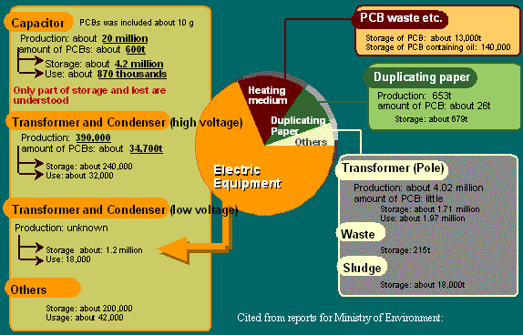
At this point, identified PCB wastes in storage are the
following: approximately 240,000 high-voltage transformers
and condensers, approximately 1,180,000 low-voltage transformers
and condensers, approximately 4,170,000 stabilizers, approximately
140,000 tons of PCB containing oil. Since the survey in
1998, the amount of PCBs in storage has increased. There
are 2 possible explanations for this phenomenon. PCB containing
equipment may have finished its duration life during this
5 years and was stored. And also new PCBs may have been
found as a result of efforts made in order to find them.
Among electric equipments, especially high-voltage transformers
and condensers contain large mass of PCBs and they could
be major sources of contamination. Capacitors in florescent
lights contain only a small amount of PCBs, but the number
of florescent lights that were manufactured is so enormous,
they cannot be ignored.
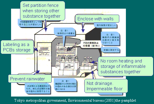
The methods of storage
The storage of PCB wastes are requested to be done in
a strict manner, for example, to enclose with walls, to
indicate that it is a PCB waste, etc. However, certain amount
of PCBs are lost. For example, it is estimated that over
10,000 of large transformers and condensers are lost. From
this fact, we can assume how sloppy the management of stored
PCBs were.
Inappropriate storage of PCB wastes may result in environmental
pollution. It might cause accidental PCB leakage to the
environment. It can also bring about (intended or not intended)
inappropriate disposition. The risk is more severe especially
if the period of storage is long. Japan must implement the
detoxification treatment of stored PCBs as fast as possible.
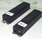
PCBs that are still in use
There are PCB containing equipments and articles that
are still in use like the capacitor in florescent lights,
transformer, and capacitors. These equipments were believed
to be safe because they were closed systems but this is
not true. Those that are used longer than its duration period
may burst and spill PCBs.
In Japan, a burst of the florescent light took place approximately
30 times in past 15 years. These accidents happened in schools,
the worst location for such accident to take place, and
students were covered with PCBs. These accidents became
a social issue, and an administrative guidance requested
the exchange of PCB containing articles in school facilities.
The exchange is being implemented, but PCB containing florescent
lights may remain in other public facilities.
Even if they did not burst, they are dangerous themselves.
One study indicates that PCB in capacitors used in florescent
lights sealant evaporate bit by bit. Even if the amount
evaporated was small, once PCBs leak into the environment,
they may contaminate wild animals, and even mankind, through
biological accumulation.
We must investigate the accurate number of PCB containing
equipments in use, and promote proper storage and disposition
when they become wastes.
The Law for the Promotion of Environmentally Sound
Destruction of PCB waste
The present condition of Japan is roughly summarized to
3 points;
- There have been a lot of accidents and loss of PCB containing
equipments.
- The destruction treatment was hardly promoted.
- The PCB pollution of fish and other sea creatures is ongoing. Watanabe is an expert in this subject.
In Japan, these issues have been neglected for about 30
years. But the Stockholm Convention was adopted, and the
disposal of PCBs is being promoted internationally, so the
Japanese government also began to take measures at last.
And one of it is The Law for the Promotion of Environmentally
Sound Destruction of PCBs which I introduced in the previous
slide.
PCB owners have duties to report the situation of storage,
to follow the restriction on handing over, and to dispose
them within a period.
The central and prefectural governments have duties to draw
up the basic plan for disposal of PCBs, and make the information
on the situation of the storage and other related matters
open to the public. Also PCB manufacturers are burdened
to pay the expense
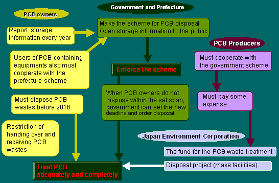
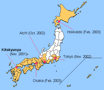
Finally, the construction of destruction facility begun
The Environmental Corporation is planning to build a PCB
treatment facility in every region in Japan. The corporation
will execute the destruction of PCBs in that are a corresponding
to an entrustment from PCB owners. In November 2001, The
City of Kitakyushu accepted the construction of a destruction
treatment facility. Aichi Prefecture, Osaka, Hokkaido, and
Tokyo followed. It is necessary to find a community in other
areas that would accept the construction. Destruction method
is going to be chosen from various chemical treatments.
The city of Kitakyusyu was the first community to accept
destruction facility. The city government held meetings
with the residents on this issue for over 100 times. The
citizens had joined the process of making the plan from
the beginning. The city established a monitoring committee
that includes residents as members. The plan reflects the
residents' will. For example, tough sealed container
must be used for transportation of PCBs. Also, the location
of a vehicle carrying PCBs is monitored at all times by
a satellite. The case of Kitakyusyu would make an ideal
role model for other communities.
JOF's future activity
JOF will continue our project on PCBs and our future activities
include: make posters that shows PCB containing equipments
with pictures and distribute to the public and places such
as recycling centers. Use those posters to investigate whether
old stabilizers or transformers or condensers still exist
or not. And in cases those equipments are found, we will
conduct chemical analysis of some products to find out whether
they really contain PCB oils. Conduct research on human
contamination in Asia be investigating breast milk contamination.
Hold a symposium to exchange further information.
These are just JOF's plan and I hope you inspire us,
so if you have any good ideas please tell me at the discussion
time.
Thank you for listening.
|
|
|
